 Victory Carries Hope
Victory Carries Hope
Victory Carries Hope

 admin
admin  2021-01-24 23:38:28
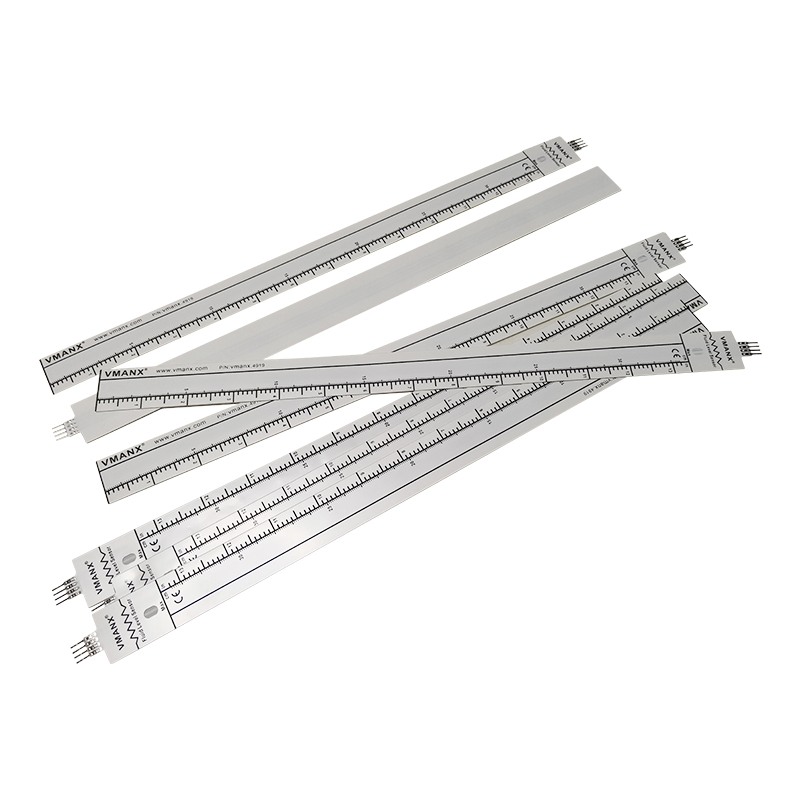
1. Design constraints
The material of LENS can be non-conductive materials such as plastic and glass, and there must be no conductive materials on it.
① Since the evaporation/sputtering nickel, chromium and alloy have metal properties, they have an impact on the sensitivity of the touch button, so we generally use non-conductive plating;
② Screen printing ink with mirror effect. This ink contains metal particles and has metal properties. Therefore, this ink will affect the sensitivity of the touch button, and should be avoided as much as possible;
③ According to the working principle of the touch button, the thickness of the covering layer is as thin as possible. Since the covering layer of the touch button is located on the surface of the product, it needs to withstand external forces. If the thickness is too thin, the strength will be insufficient, so the ideal thickness of the covering layer is 1.0- Between 3.0mm;
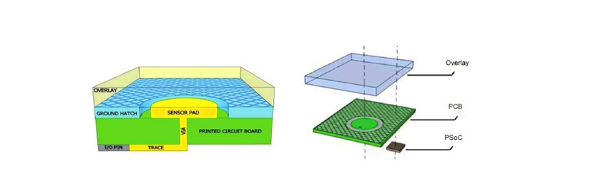
④ The dielectric constant of air is 1, and the dielectric (air) is more easily polarized by the applied electric field. Air will greatly affect the sensitivity of touch buttons, so the assembly of double-sided tape is also a key process in the production and assembly of touch buttons.
⑤ The distance between two sensors should not be less than 3mm (the distance between two adjacent keys is greater than the thickness of the panel);
⑥ The size of the sensor should not be less than 10mm*10mm;
⑦ Generally round and square with rounded corners are commonly used for sensors, but special shapes such as triangles are not recommended;
⑧ The recommended distance between the sensor and the reference ground is 0.5mm-2mm;
⑨ The edge of the button should not be less than 3.5mm from the edge of the panel;
⑩ The sensor lead should not be too close to the interference source (large current, high frequency signal).

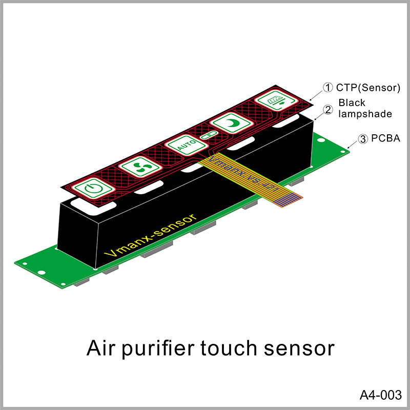
2. Application structure
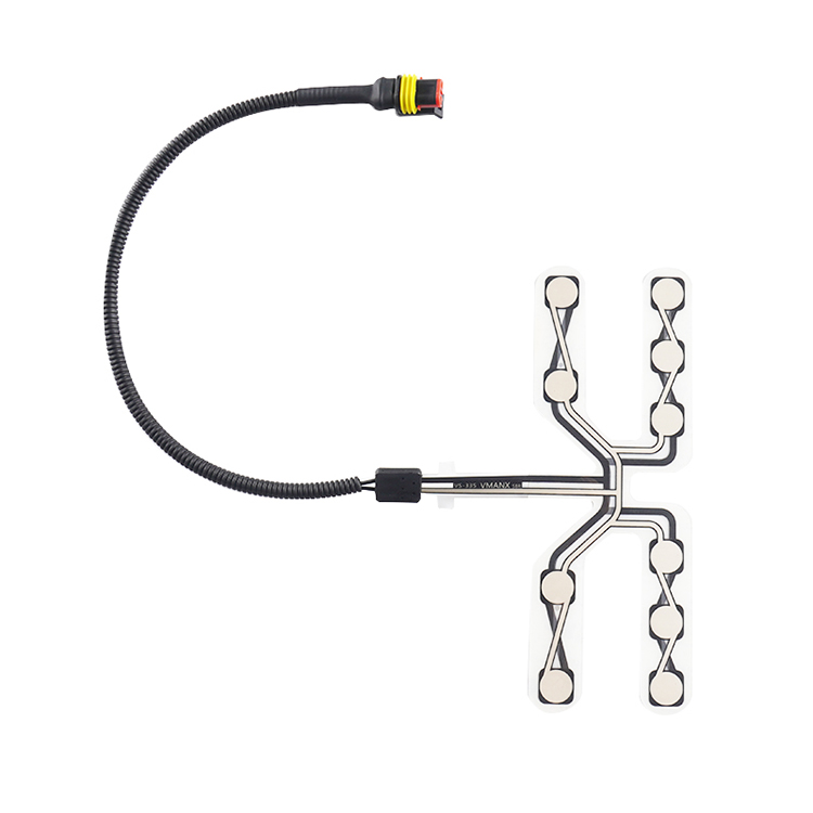
(1). Copper foil coupling electric field (a PCB-based design method)
1. Directly use the copper foil etched on the PCB surface as a sensor, low cost;
2. The electric field is emitted from the copper foil sensor and points to the ground plane;
3. Do not use mechanical moving parts, use an insulating covering as the touch surface of the button;
4. Simplified structure, ideal plan for pure flat panel design.
(2) Coupling the electric field through a spring (a PCB-based design method)
1. The electric field is coupled from the PCB to the cover layer through the compression spring;
2. Use conductive material as the connection point of the capacitive sensor;
3. No mechanical moving parts are used, and the spring does not move;
4. The ideal method to avoid the use of double-sided adhesive bonding process.

3. Slider touch circuit design
Knob Pad: Combine multiple touch pads to form a scroll wheel, which can be used with IC to detect the direction and position of the finger sliding; when the finger is moving on the slider, two adjacent
The electrode change is opposite. The electrode with stronger signal is the position where the finger is about to reach, and the electrode with weaker signal is the position of the electrode where the finger is about to leave